
Welcome to the world of PCB manufacturing, where precision meets innovation to power our electronic devices. In this comprehensive guide, we’ll delve into the intricate process of creating printed circuit boards (PCBs) from the initial design stages to the final assembly, exploring key concepts, best practices, and the latest technologies shaping this dynamic industry.
Understanding PCB Design
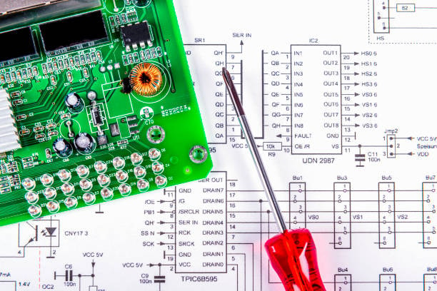
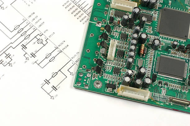
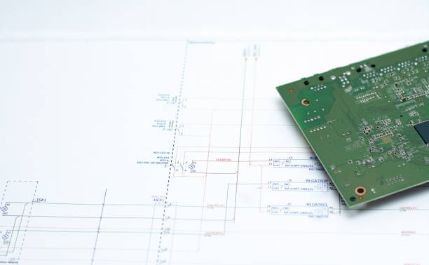
The journey begins with PCB design, a crucial phase that lays the foundation for a successful manufacturing process. Design engineers leverage sophisticated software to create schematics, define component placement, and establish signal paths. Factors like trace routing, layer stack-up, and component selection are meticulously optimized to meet performance, size, and cost requirements.
What is the PCB Manufacturing Process?
The PCB manufacturing process involves several key steps that transform a design into a functional printed circuit board ready for electronic components. Here’s a simplified breakdown:
Designing the PCB
Engineers use specialized software to create the PCB layout, including component placement, trace routing, and layer stack-up.
Material Selection
Choosing the right substrate material (e.g., FR-4, ceramic, flex) and copper thickness based on performance and application requirements.
Laying Copper and Etching
Layers of copper foil are laminated onto the substrate. A chemical etching process removes excess copper, leaving behind the desired circuit traces.
Drilling Holes
Holes for through-hole components and vias are drilled using precision drilling machines. Vias connect different layers of the PCB.
Plating and Surface Finish
Copper surfaces are plated to enhance conductivity and protect against oxidation. Surface finish options include HASL, ENIG, OSP, and immersion silver.
Solder Mask Application
A solder mask is applied over the PCB to insulate traces and pads, except where components will be soldered.
Silkscreen Printing
Component labels, logos, and reference indicators are printed on the PCB using a silkscreen process.
Component Placement
Automated assembly machines or manual labor place surface-mount components (SMDs) on the PCB using solder paste.
Soldering
The PCB passes through a reflow oven where solder paste melts, creating electrical connections between components and PCB traces.
Testing
Automated optical inspection (AOI), X-ray inspection, and functional tests check for defects, soldering quality, and overall functionality.
Final Inspection and Packaging
PCBs that pass testing undergo final inspection before being packaged and prepared for shipment to customers or assembly into electronic devices.
What are the Parts of a PCBs?

Certainly! Here’s a breakdown of the main parts of a printed circuit board (PCB):
Substrate/Base Material
The substrate, also known as the base material, forms the foundation of the PCB. It is typically made of fiberglass-reinforced epoxy laminate (FR-4) due to its excellent electrical insulation properties and mechanical strength. Other materials like ceramic, polyimide (flex PCBs), and metal core substrates are also used for specialized applications.
Copper Layers
Copper layers are thin sheets of copper foil laminated onto the substrate. These layers form the conductive pathways (traces) that carry electrical signals between components on the PCB. The copper thickness is specified in ounces (e.g., 1 oz, 2 oz) and affects the PCB’s current-carrying capacity and impedance.
Solder Mask

The solder mask is a protective layer applied over the copper traces to prevent accidental short circuits and oxidation. It is usually green in color (although other colors are used for aesthetic or functional purposes) and is non-conductive. Openings in the solder mask allow soldering of components to the copper traces.
Silkscreen/Component Legend
The silkscreen layer contains component labels, reference designators, logos, and other markings that aid in component placement and assembly. It is typically printed in white ink on top of the solder mask, providing visual guidance during PCB assembly and troubleshooting.
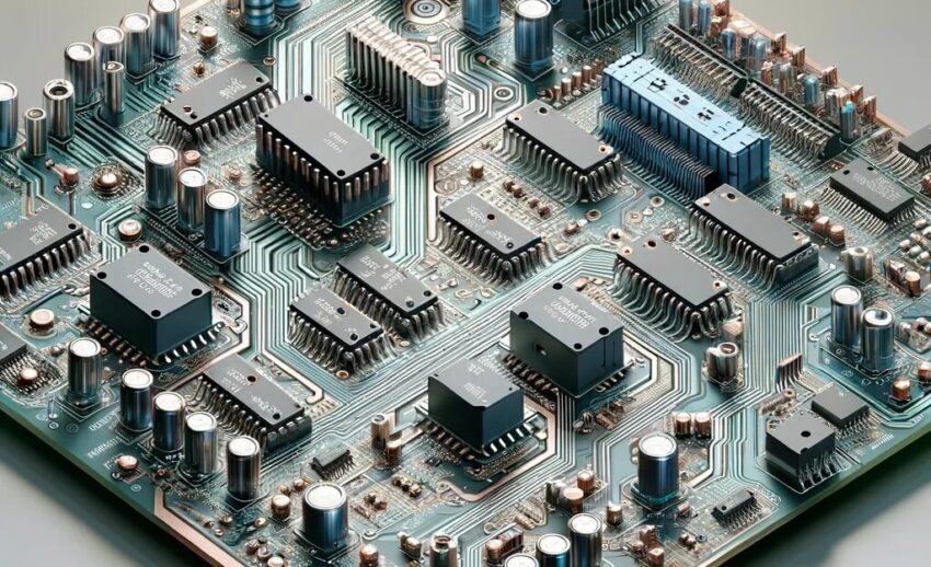
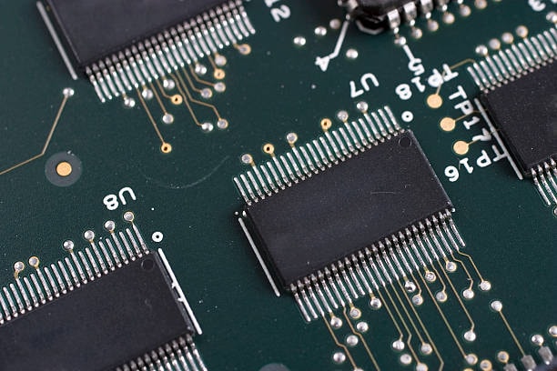
Components
Components are the electronic parts mounted on the PCB to perform specific functions. They can be categorized into two main types:
- Through-Hole Components: These components have leads that pass through holes drilled in the PCB and are soldered on the opposite side. Through-hole components include resistors, capacitors, diodes, and some connectors.
- Surface Mount Components (SMDs): SMDs are mounted directly onto the surface of the PCB, typically using solder paste and reflow soldering techniques. They are smaller in size and include ICs (integrated circuits), microcontrollers, LEDs, and surface-mount resistors/capacitors.
Vias
Vias are plated-through holes that connect different copper layers of the PCB. They allow electrical signals to pass vertically through the board, enabling complex multi-layer PCB designs. Vias can be through-hole vias (THT) or surface-mount vias (SMD) depending on their placement and purpose.
Pads and Traces

Pads are areas of exposed copper on the PCB surface where components are soldered. Traces are conductive pathways that connect pads and components, forming the electrical circuitry of the PCB. Trace width, spacing, and routing configurations are critical for signal integrity, impedance control, and thermal management.
How is a PCB Manufactured?
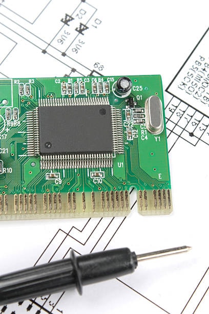
The manufacturing of a printed circuit board (PCB) involves several sequential processes that transform a design into a functional electronic component carrier. Here is an overview of the typical steps involved in PCB manufacturing:
Design Preparation
The process begins with the preparation of the PCB design files using specialized software. This includes creating the schematic, laying out components, defining trace routes, and specifying layer stack-ups.
Material Selection
Once the design is finalized, the appropriate materials are selected. This includes choosing the base substrate material (commonly FR-4), copper foil thickness, and solder mask type based on the design requirements and application.
Board Preparation
The base material is cut into standard sizes, and copper foil is laminated onto both sides of the substrate. This forms the copper layers that will later become the conductive traces on the PCB.
Imaging and Etching
The PCB design is transferred onto the copper-clad substrate using a process called imaging. A photoresist layer is applied to the copper surface, and the design pattern is transferred using UV light. The unexposed areas are then removed using a chemical etching process, leaving behind the desired copper traces.
Drilling

Holes are drilled into the PCB to accommodate through-hole components and vias. Automated drilling machines with high precision are used to ensure accuracy in hole placement.
Plating
After drilling, the exposed copper surfaces inside the holes and on the PCB’s surface are plated with a thin layer of metal (typically copper) to enhance conductivity and prevent oxidation.
Solder Mask Application
A solder mask layer is applied over the PCB, covering all areas except where components will be soldered. This layer is typically green in color but can be customized for aesthetic or functional purposes.
Silkscreen Printing
Component labels, reference indicators, logos, and other markings are printed onto the PCB surface using a silkscreen process. This helps in component identification and assembly.
Component Placement
Automated assembly machines or manual labor is used to place surface-mount components (SMDs) onto the PCB. Solder paste is applied to the pads, and components are placed using pick-and-place machines.
Soldering
The PCB passes through a reflow oven where the solder paste melts and creates strong electrical connections between components and PCB traces. For through-hole components, wave soldering or selective soldering techniques are used.
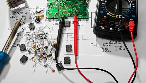
Testing and Inspection
After soldering, the PCB undergoes various tests and inspections to ensure functionality, quality, and reliability. This includes automated optical inspection (AOI), X-ray inspection, functional testing, and electrical testing.
Final Finishing
Once the PCB passes testing, final finishing processes are carried out. This may include applying a surface finish (e.g., HASL, ENIG, OSP), edge plating, and final inspection before packaging and shipping.
Material Selection and Stack-Up
Material selection and stack-up are critical aspects of PCB manufacturing that directly impact the board’s performance, reliability, and functionality.
The process begins with choosing the appropriate substrate material, often fiberglass-reinforced epoxy laminate (FR-4), due to its excellent electrical insulation properties, mechanical strength, and cost-effectiveness. However, for specialized applications requiring specific properties like high-frequency performance or flexibility, materials such as ceramic, polyimide (flex PCBs), or metal core substrates may be selected.
Once the substrate material is determined, the next step is to decide on the number of copper layers and their thicknesses. The stack-up configuration defines the arrangement of copper layers, signal layers, power planes, and ground planes within the PCB. Thicker copper layers are used for higher current-carrying capacity and better heat dissipation, while thinner layers offer more flexibility in routing and lower manufacturing costs.
Additionally, the choice of copper weight (measured in ounces per square foot) influences the PCB’s impedance, signal integrity, and thermal characteristics. Common copper weights include 1 oz, 2 oz, and 3 oz, with higher weights providing increased current handling capabilities but requiring careful consideration of trace widths and spacing to avoid impedance mismatches.
Fabrication and Copper Etching
Fabrication in PCB manufacturing involves laminating copper layers onto the substrate and etching away excess copper to form the desired circuit traces. The process starts with applying a layer of copper foil to the substrate, followed by photoresist application and exposure to UV light using the PCB design. Areas not protected by the photoresist are etched away using chemicals, leaving behind the circuit traces that define the electrical pathways on the PCB. This step is crucial for ensuring accurate signal transmission and proper functionality of the final electronic device.
SMT and Through-Hole Assembly
SMT (Surface Mount Technology) and Through-Hole Assembly are two common methods used to mount electronic components onto printed circuit boards (PCBs).
And SMT involves placing components directly onto the surface of the PCB, where solder paste is applied to the pads beforehand. The PCB then goes through a reflow soldering process, where heat melts the solder paste, creating a strong electrical connection between the components and the PCB. This method is widely used for its space-saving advantages, allowing for smaller and more densely populated PCBs.
On the other hand, Through-Hole Assembly involves inserting component leads through pre-drilled holes in the PCB. The leads are then soldered on the opposite side of the board, forming secure mechanical and electrical connections. Through-hole components are often used for their durability, especially in applications requiring robust mechanical support or high current-carrying capacity.
Both SMT and Through-Hole Assembly have their strengths and are often used together in mixed-technology PCBs to optimize performance and functionality based on component requirements and design considerations.
Quality Assurance and Testing
Quality assurance and testing are crucial phases in the PCB manufacturing process to ensure that the final product meets the required standards of functionality, reliability, and performance.
And quality assurance starts early in the process with thorough checks during material selection, stack-up design, and fabrication. Once the PCBs are manufactured, they undergo a series of tests to identify any defects or issues that could affect their performance.
Automated Optical Inspection (AOI) is commonly used to visually inspect the PCBs for defects such as soldering errors, component misalignment, or missing components. AOI systems use cameras and image processing algorithms to detect abnormalities and ensure that the PCBs meet the specified design criteria.
X-ray inspection is another essential tool for inspecting the internal structure of PCBs, especially for detecting defects like hidden solder joints, voids, or delamination. X-ray systems provide detailed images of the PCB’s internal layers, allowing for thorough analysis and verification of quality.
Functional testing is performed to verify that the PCB operates as intended and meets the functional requirements specified in the design. This may include testing electrical connectivity, signal integrity, power distribution, and compatibility with other electronic components or systems.
In addition to automated testing, manual inspections and in-circuit testing (ICT) may also be conducted to ensure comprehensive quality assessment. ICT involves testing individual components and circuits on the PCB to validate their functionality and performance.
Industry Trends and Innovations
As technology evolves, so does the landscape of PCB manufacturing. Trends like additive manufacturing (3D printing), flexible electronics, and embedded components are reshaping how PCBs are designed and produced. Emerging concepts like IoT integration, AI-driven design optimization, and sustainable manufacturing practices pave the way for a smarter, greener future.
Conclusion: Advancing Electronics Through PCB Mastery
Mastering the art of PCB manufacturing is a blend of technical expertise, creative design, and continuous innovation. From concept to reality, each step in the process contributes to the seamless integration of electronics into our daily lives. As we embrace new challenges and embrace cutting-edge technologies, the journey of PCB manufacturing continues to inspire, drive, and transform the world of electronics.
Summary
Mastering the art of PCB manufacturing encompasses a meticulous journey from initial design to final assembly. It begins with meticulous design preparation, where engineers utilize specialized software to create schematics, define component placement, and establish trace routes. Material selection plays a pivotal role, determining the substrate material, copper thickness, and solder mask type based on performance requirements. The fabrication process involves precise imaging and etching to form circuit traces, followed by drilling for component insertion. Plating and surface finishing ensure optimal conductivity and protection against oxidation. Assembling components, whether through surface mount technology (SMT) or through-hole methods, demands precision and adherence to design specifications. Quality assurance and testing processes, including automated optical inspection (AOI) and functional testing, validate PCB integrity and functionality before final deployment.
The culmination of these processes results in high-performance printed circuit boards (PCBs) that underpin modern electronics. From consumer devices to industrial applications, PCBs serve as the backbone of electronic systems, enabling seamless connectivity and functionality. Mastering PCB manufacturing requires a blend of technical expertise, creative design, and stringent quality control, ensuring that each board meets the rigorous standards of reliability, performance, and durability demanded by today’s technology-driven world.